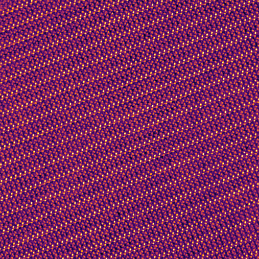
Guide: Indexing Diffraction Patterns with Vector Graphics Overlay
Published:
We will use ReciPro (Paper) to index a selected-area electron diffraction (SAED) pattern of a GaAs single crystal to find the zone axis.
Then, this guide will show how to overlay the diffraction spots onto the experimental image as vector graphic using Inkscape as shown below:
Download example data files.
Step 1: Inspecting the Diffraction Pattern
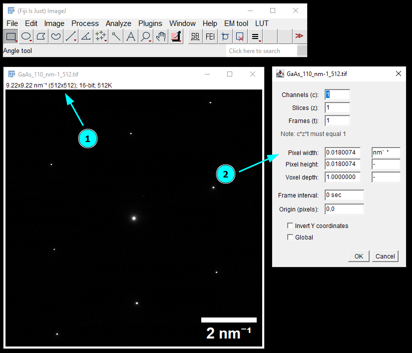
First, let’s open the tif image in Fiji to inspect it. Here, we see that the image is already calibrated in inverse nm and has 512x512 pixels (1). Using Image -> Properties…, we can find the pixel size of 0.0180074 1/nm (2). Here, we assume this calibration is correct. We will need to this value in a moment and leave the window open.
Note: This tutorial works similarly for FFTs/Power Spectra. Only make sure that the FFT spots are nicely distringuishable above the background.
Step 2: Open ReciPro and Spot ID
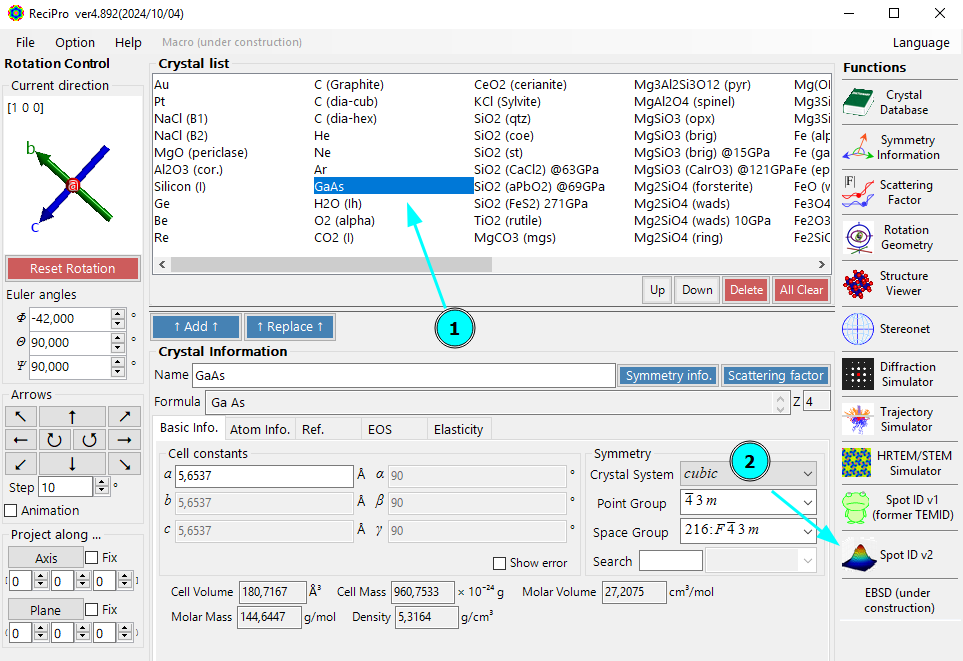
Next, we open ReciPro. In this example, we know our sample (GaAs) and can therefore select it from the built-in crystal structures (1). You can load your own cif files to add different crystal structures to ReciPro.
We start the Spot ID (v2) module for diffraction-pattern indexing (2).
Step 3: Load the Diffraction Pattern and Adjust the Calibration
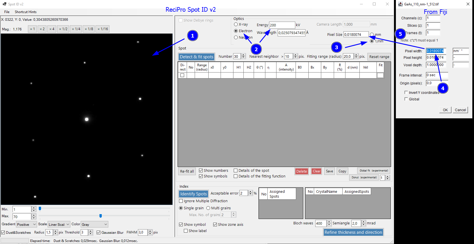
Drag and drop the tif image of the SAED pattern into the left side of the Spot ID window (1) (or use File -> Read). This should open the diffraction pattern. Below the image, you can adjust the intensity display for better visibility of the spots if desired.
Next, we can set the experimental parameters to Optics -> Electron and Energy to 200 kV to match the experiment. Next, we set the pixel size in 1/nm (3). My ReciPro installation uses comma instead of a point as decimal sign (might be my German Windows setup). Before copying the value, I change the decimal sign to comma in Fiji (4) and then copy it to ReciPro (5). Now the image is scaled. Do not adjust the Energy value after setting the pixelsize as it modifies the scaling.
Step 4: Fit the Diffraction Spots
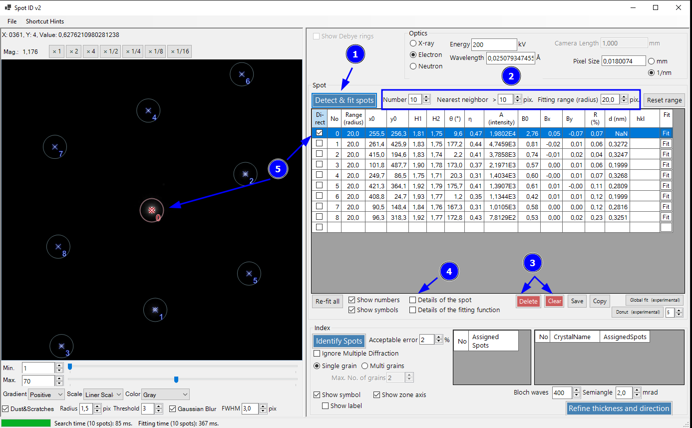
Now we fit the diffraction spots using Detect & fit spots (1). If the fit is not good, play around with the values in the box (2). Here, we only reduced the maximum number of spots from 30 to 10 and left the rest default. All 9 spots are nicely detected (indexed in blue).
In case you have to few/many peaks, you can clear the current spot list (3) and try again with different parameters (2). You can also inspect the each individual fit by selecting the spot and clicking Details of the spot (4).
Finally, we can set the direct beam from the list (5), which automatically done correctly here by ReciPro (indexed in red).
Step 5: Check the Database for the Crystal Phase and Orientation
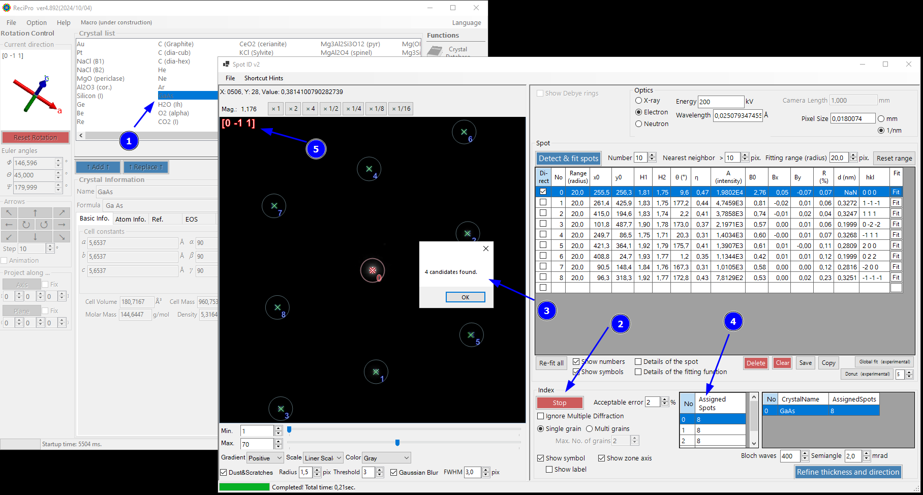
Select a crystal structure (here GaAs) from the list in the ReciPro main window (1), then hit Identify spots (2). ReciPro will show a message (3) and - if any orientation and crystal structure matches - will populate a list of possible orientations (4). Typically, the higher the number of assigned spots, the better is the match with the experimental pattern. The zone axis suggestion is shown in the top-left corner of the diffraction pattern (5). The expected spot positions are overlaid as green. Here, it shows a good match with the experimental spot positions in blue. You can play around with the options in the Index menu if the fit to your experimental pattern is not good. For example, strain or miscalibration of the pixel size might require a higher Acceptable error value.
If all you wanted is checking the orientation and phase (here GaAs<0-11>), you are already done here! :-)
You can save the result as png and emf using File -> Save.
Step 6: Simulate the Diffraction Pattern under the same Conditions
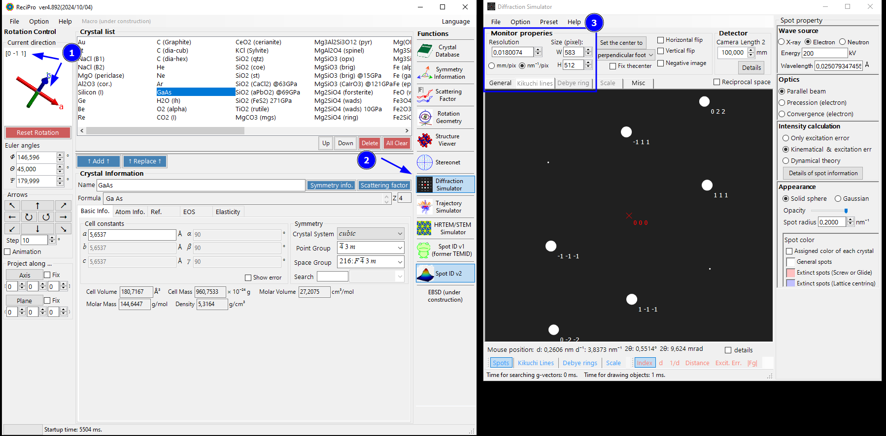
We now continue to prepare a nice vector graphic with the indexing results overlaid on the experimental SAED pattern. First, notice that the selected, indexed orientation from Spot ID window is carried over to the main window and the crystal orientation is the same (1). Do not modify it!
Instead, we open the Diffraction Simulator window. Here we need to be careful with correctly scaling the simulated diffraction pattern so that it matches our experiment.
Ideally, you can set the same pixel dimension (512x512) and pixel size (0.0180074 1/nm) as the experimental pattern (3). However, the pixel size you can set in the diffraction simulator depends also on the displayed GUI-element size and your monitor. For example, Here, it is not possible to set a width of 512 on a 1080p monitor as the GUI elements will not permit it.
This is not a big problem, since we scale the vector graphics file in the end anyway. To make it simple, we want to keep a square aspect ratio (width=height). Depending on your monitor, you can try to set 1024x1024 as the size with half the pixel size (0.5 * 0.0180074 1/nm). For my 1080p monitor, this integer scaling will not work as 1024 is too big.
As a solution for our monitor, we choose 700x700 pixel and set the pixel size to 512/700 * 0.0180074 1/nm = 0.0131711269 1/nm (note that I used comma as decimal sign in ReciPro).
Step 7: Adjusting the Spot Appearance and Export to emf
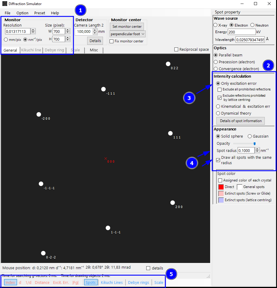
After setting up the correct pixel size (1), we can do an initial change of the appearance of the spots and diffraction pattern (2). For a simple indexing of the spot positions (and not their intensities), we only want simple geometric spots. We can get this by selecting Only excitation error (3), Draw all spots with the same radius (4). I also reduced the spot radius a bit (4). At the bottom of the window, we can adjust the information shown in the diffraction pattern (5). We keep the Miller indices in this example (=Index option).
Finally, we save the pattern as emf vector graphic using File -> Save -> as Metafile.
Note: You may see an unwanted “fade out” of the spots for your own diffraction patterns depending on the reciprocal range. If you want to prevent this, increase the Energy value on the top right.
Step 8: Use Inkscape to Overlay the Spots
We just prepared the emf for the simulated diffraction pattern. It is best to also save the experimental pattern as a vector svg file, e.g., by using BioVoxxel-Figure-Tool’s svg export. An svg is provided for this example (DiffPattern_log.svg), which we can open in Inkscape. Note that the intensity was log-scaled for a better visibility of the spots. Open also the emf in the same Inkscape window.
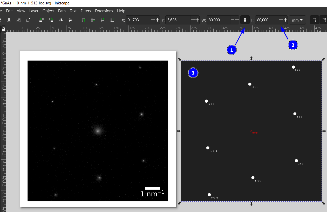
Lock the aspect ratio (1) and change the image to the same size, e.g., 80 mm by 80 mm in this example.
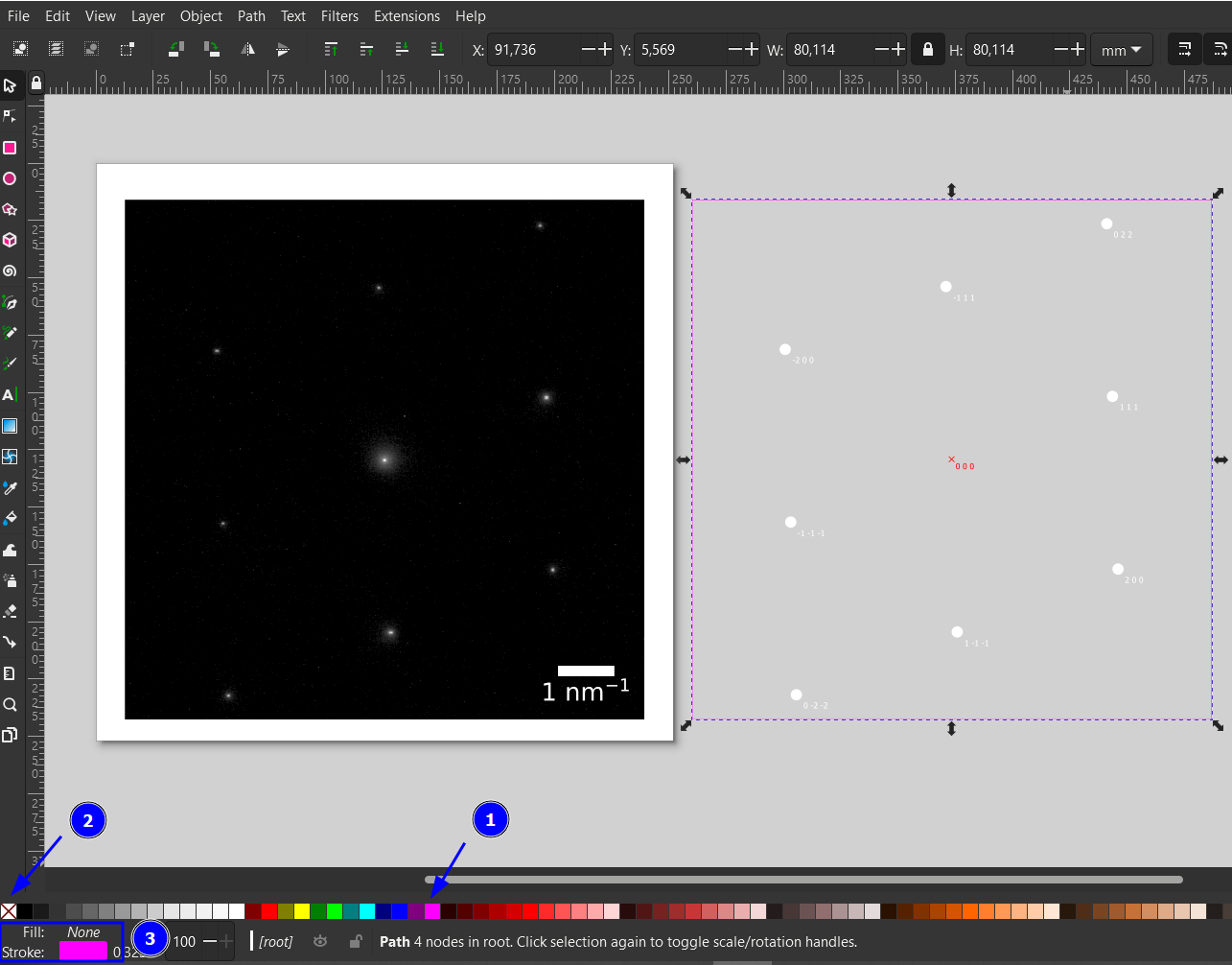
Select the simulated diffraction pattern, and Ungroup (Ctrl+Shift+G) the elements. Click on the black background but don’t move it. We temporarily give it a stroke for reference (Crtl+left-click on the color, here in fuchsia color, see 1) and then remove the fill (2). This leaves us with a fuchsia-colored frame and the spots. Select the frame and all elements of the simulated pattern and group it (Ctrl+G).
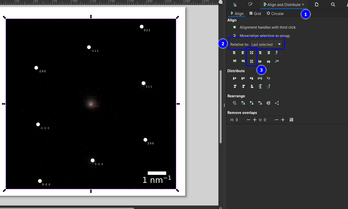
Move the diffraction pattern on top of the experimental pattern. This can be done either by dragging or the Align and Distribute menu (Ctrl+Shift+A, 1). Depending on the settings (2), you need to select the two elements while holding shift in a specific order. Here, we first Shift+Click on the simulated pattern and then the experimental and then use Relative to: Last Selected combined with the two align operations in (3).
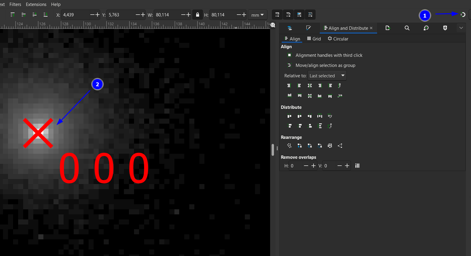
We would be done with the alignment if the direct beam would be perfectly centered in the experimental pattern. This is often not the case and we have to move the simulated pattern a bit to match the direct-beam position and the red cross. It is good to temporarily switch off the “snapping” for this operation (1). Zoom into the center to carefully align the patterns (2).
Now the patterns are aligned! :-)
Step 9: Modify the Spot Apperance
Now we can modify the appearance of the spots. Here, we want to show the original experimental spots with the simulated positions as yellow circles around them.
In a first step, zoom out, select the simulated pattern (click on a spot), and ungroup it (Ctrl+Shift+G).
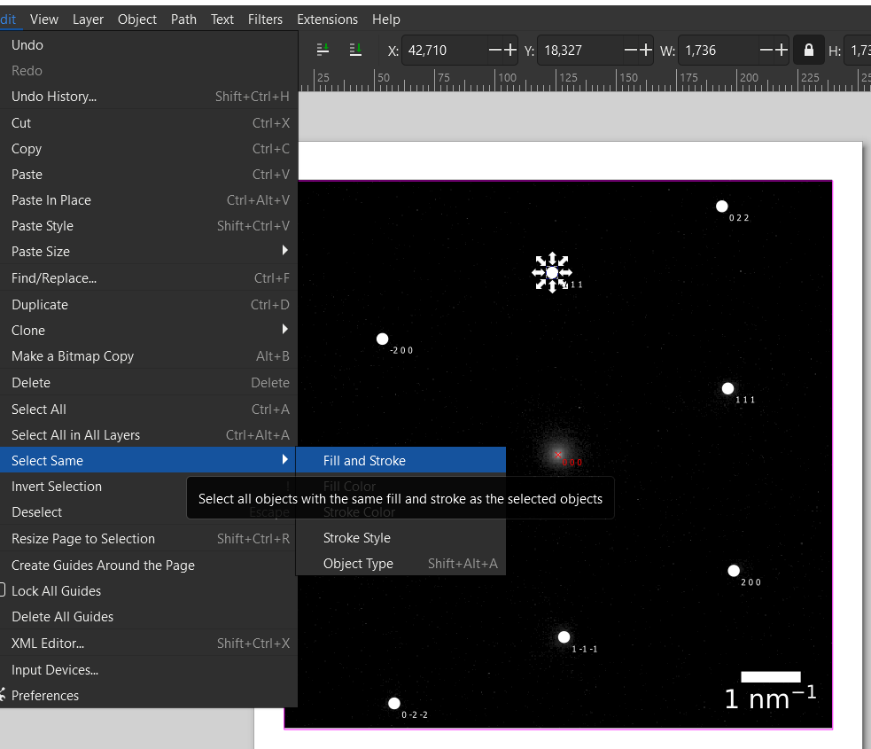
Now we need to select all spots. In this example with only 9 diffraction spots, we could do this by Shift+left-click on each spot. However, for more spots this gets too tedious. Instead, we click on one spot and then use Edit -> Select Same -> Fill and Stroke. This typically works to select all diffraction spots.
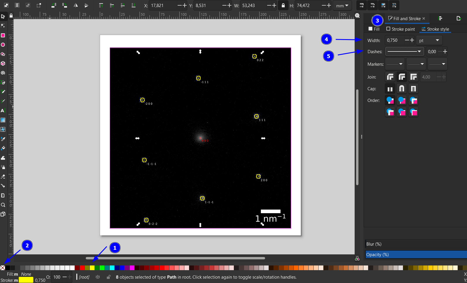
We now apply a yellow stroke (Shift+click on yellow, 1), remove the filling of the spots (click on 2). We increase the stroke line width to 0.750 pt (4) from the Stroke and Fill menu (Ctrl+Shift+F, 3). Here, you could also change the stroke style, e.g., dashed (5).
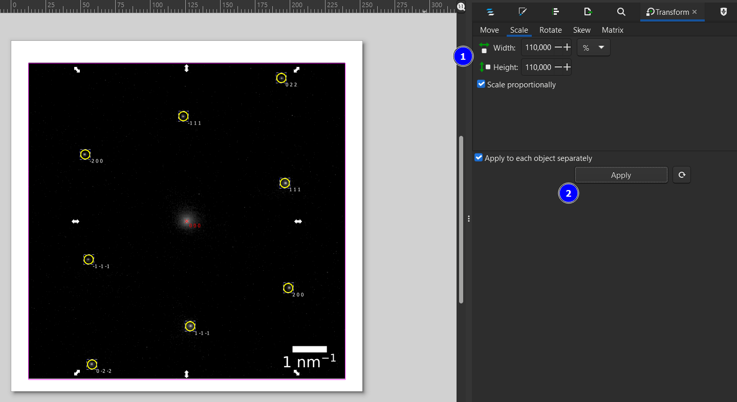
Next, we increase the circle radius a bit using the Scale transformation in the Transform menu (Ctrl+Shift+M, 1). I set it here to 110% and hit apply a few times (2) until the circles have the desired size. This will also scale the stroke width, which can be set back manually similar to the previous step (Stroke and Fill menu).
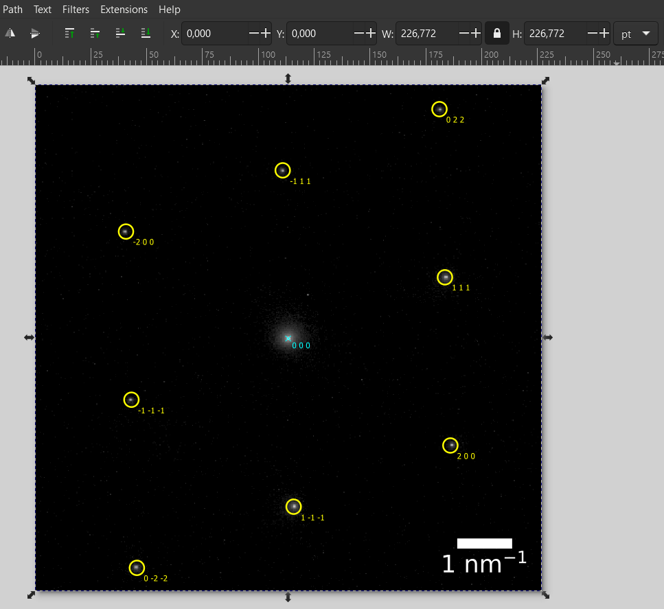
You can proceed to modify the rest of the overlay to your desire. Here, we select the Miller indices from the spots and give them also a yellow fill. The direct beam was changed to cyan.
Finally, we select all spots by drag-selection with the mouse and then Shift+Click on the experimental pattern to select all elements. We group them (Shift+Group) and also Edit -> Resize Page to Selection (Ctrl+Shift+R) to remove/hide the white border. This will yield the final result below.
You can now save this pattern to different formats (svg,pdf) or export to rasterized images (Ctrl+Shift+E).
Recap
In this tutorial we used ReciPro to find a crystal orientation and simulate the diffraction-spot positions. From ReciPro, we can save the simulated positions to a vector graphic file and overlay the simulated spot positions onto the experimental pattern.
Thanks for reading and happy pattern indexing!
Additional credits:
Screenshots were made with Flameshot.
